This blog was originally posted at Fortune.
Semiconductors have transformed virtually every aspect of our lives. Now, the semiconductor industry is on the verge of a profound transformation itself.
Customized silicon—chips uniquely tailored to meet the performance and power requirements of an individual customer for a particular use case—will increasingly become pervasive as data center operators and AI developers seek to harness the power of AI. Expanded educational opportunities, better decision making, ways to improve the sustainability of the planet all become possible if we get the computational infrastructure right.
The turn to custom, in fact, is already underway. The number of GPUs—the merchant chips employed for AI training and inference—produced today is nearly double the number of custom XPUs built for the same tasks. By 2028, custom accelerators will likely pass GPUs in units shipped, with the gap expected to grow.1
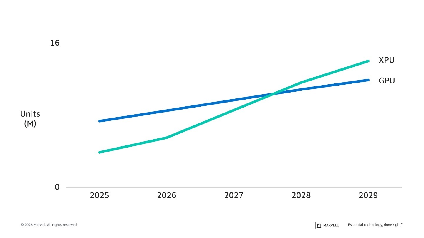
Custom AI accelerators are expected to pass GPUs in unit shipments during the decade while costing substantially less. Source: Dell’Oro Group
Custom designs will also increasingly extend into other categories. Custom network interface controllers (NICs)—which act as gateways from individual systems to the broader network—already constitute more than 30% of NICs inside the infrastructure of some of the largest data center operators2. Even very high-volume devices like storage controllers will increasingly be bespoke. New devices such as CXL controllers, which add massive amounts of memory or compute cores to systems, are debuting as custom products before or at the same time as their merchant counterparts.
Moore’s Law and More Data Centers
For decades, semiconductor makers relied on Moore’s Law, i.e., dramatically reducing the size of the transistors inside their chips, to boost power, performance, and value. It worked fantastically. I started my career working on the Pentium Pro. A breakthrough design at its time, the chip contained 5.5 million transistors.3. Now, the largest chips contain over 200 billion transistors. One trillion transistor devices with multiple layers of silicon are expected toward the end of the decade.4
Unfortunately, the gains in power and performance achievable through transistor scaling have dramatically slowed. Chip development and manufacturing costs have also continued to rise: Designing a leading-edge processor can now cost over $300 million5.
At the same time, AI models have been evolving rapidly, demanding 2x more compute power every few months, faster than the two-year upgrade cycles of the past. Demand for digital services, meanwhile, has continued to rise, further fueling the need for data center capacity.
These converging trends mean that, without dramatic changes, AI becomes more expensive and resource-intensive. Data center electricity consumption, historically around 1-2% of the worldwide total,6 now threatens to reach 6-12% of total U.S. electricity consumption by 2028.7 In data center hubs like Ireland, data centers already consume 21%, fueling community objections.8
The Custom Cookbook
Customization essentially complements increasing transistor density with design creativity. Engineers are rethinking established principles to unearth unexpected gains.
Consider high-bandwidth memory (HBM), a relatively new class of memory placed alongside AI processor cores. The more HBM developers can include, the greater the potential performance. Adding GBs of HBM, however, adds power and cost: approximately 30% of the material cost of an accelerator can be memory.9 By customizing the base die—an unheralded chip that serves the interface between the computing cores and memory—the silicon footprint for HBM gets slashed. The result: room for up to 33% more memory storage capacity, interface power reduced by up to 70% and 25% more room for computing cores.
Likewise, an effort to customize SRAM, a faster type of memory integrated directly into the computing silicon, could boost data throughput by up to 17x—accelerating workloads, reducing time to completion and ultimately improving infrastructure return on investment. Customized/optimized silicon can also reduce downtime or streamline security tasks.
Semi Business 2.0?
The shift will also transform how semiconductor companies operate. Designing custom chips is far different than producing vast volumes of identical merchant devices and combines elements of a product business and a services firm. Companies will need to broaden their IP portfolios. Expertise in esoteric areas such as SerDes (serializer/deserializer) and die-to-die interfaces—think of these as capillaries that rapidly move data between chips or different regions within the same chip--will become disproportionately important.
Collaboration between companies will also become more prevalent. Today, the chips that convert high-voltage current from a power socket into the low voltages needed by computers sit at a considerable distance from processing cores. An emerging class of chip packaging will enable designers to place power semiconductors next to computing cores, cutting transmission losses by up to 85%. Likewise, expect to see cooperation between optical experts, cable vendors and processors and designers on the effort for co-packaged optics. Many, if not most, of these creative design efforts will also be grounded in standards to ensure innovation and cooperation across ecosystems. Custom, in other words, won’t mean incompatibility or isolation.
AI will also be deployed to cut verification time and testing from months to hours.
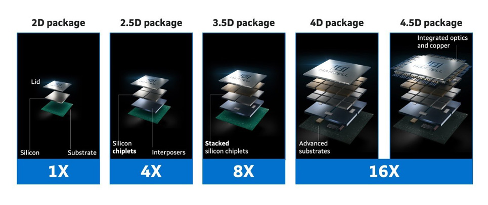
Once an afterthought, advanced chip packaging is now crucial for increasing performance count by allowing designers to insert more transistors and new functionalities into devices.
A Firm Foundation
Titanic shifts in our relationship to computing always start with silicon. The consumer internet took off after a new generation of server and desktop CPUs made it possible for almost anyone to become a consumer or producer of content online. Mobile took flight after a focus on energy efficiency processors that could provide an all-day battery life. Through custom silicon, we can turn AI from an interesting phenomenon to a springboard for human creativity.
1. Dell’Oro Data Center and IT Semiconductor Forecast, July 2025.
2. 650 Group NIC Data, July 2025.
3. Wikipedia, Pentium Pro
4. Marvell Custom AI Investor Event, June 2025.
5. IBS, 2023.
6. Science, February 2020
7. Lawrence Berkeley Laboratory and Dept of Energy, December 2024.
8. The Guardian, June 2024.
9. Marvell Average of industry analyst estimates.
# # #
This blog contains forward-looking statements within the meaning of the federal securities laws that involve risks and uncertainties. Forward-looking statements include, without limitation, any statement that may predict, forecast, indicate or imply future events or achievements. Actual events or results may differ materially from those contemplated in this blog. Forward-looking statements are only predictions and are subject to risks, uncertainties and assumptions that are difficult to predict, including those described in the “Risk Factors” section of our Annual Reports on Form 10-K, Quarterly Reports on Form 10-Q and other documents filed by us from time to time with the SEC. Forward-looking statements speak only as of the date they are made. Readers are cautioned not to put undue reliance on forward-looking statements, and no person assumes any obligation to update or revise any such forward-looking statements, whether as a result of new information, future events or otherwise.