
By Michael Kanellos, Head of Influencer Relations, Marvell
Chiplets—devices made up of smaller, specialized cores linked together to function like a unified device—have dramatically transformed semiconductors over the past decade. Here’s a quick overview of their history and where the design concept goes next.
1. Initially, they went by the name RAMP
In 2006, Dave Patterson, the storied professor of computer science at UC Berkeley, and his lab published a paper describing how semiconductors will shift from monolithic silicon to devices where different dies are connected and combined into a package that, to the rest of the system, acts like a single device.1
While the paper also coined the term chiplet, the Berkeley team preferred RAMP (Research Accelerator for Multiple Processors).
2. In Silicon Valley fashion, the early R&D took place in a garage
Marvell co-founder and former CEO Sehat Sutardja started experimenting with combining different chips into a unified package in the 2010s in his garage, according to journalist Junko Yoshida.2 In 2015, he unveiled the MoChi (Modular Chip) concept, often credited as the first commercial platform for chiplets, in a keynote at ISSCC in February 2015.3
The first products came out a few months later in October.
“The introduction of Marvell’s AP806 MoChi module is the first step in creating a new process that can change the way that the industry designs chips,” wrote Linley Gwennap in Microprocessor Report.4
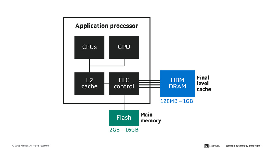
An early MoChi concept combining CPUs, a GPU and a FLC (final level cache) controller for distributing data across flash and DRAM for optimizing power. Credit: Microprocessor Forum.
Copyright © 2026 Marvell, All rights reserved.