
Chiplets—devices made up of smaller, specialized cores linked together to function like a unified device—have dramatically transformed semiconductors over the past decade. Here’s a quick overview of their history and where the design concept goes next.
1. Initially, they went by the name RAMP
In 2006, Dave Patterson, the storied professor of computer science at UC Berkeley, and his lab published a paper describing how semiconductors will shift from monolithic silicon to devices where different dies are connected and combined into a package that, to the rest of the system, acts like a single device.1
While the paper also coined the term chiplet, the Berkeley team preferred RAMP (Research Accelerator for Multiple Processors).
2. In Silicon Valley fashion, the early R&D took place in a garage
Marvell co-founder and former CEO Sehat Sutardja started experimenting with combining different chips into a unified package in the 2010s in his garage, according to journalist Junko Yoshida.2 In 2015, he unveiled the MoChi (Modular Chip) concept, often credited as the first commercial platform for chiplets, in a keynote at ISSCC in February 2015.3
The first products came out a few months later in October.
“The introduction of Marvell’s AP806 MoChi module is the first step in creating a new process that can change the way that the industry designs chips,” wrote Linley Gwennap in Microprocessor Report.4
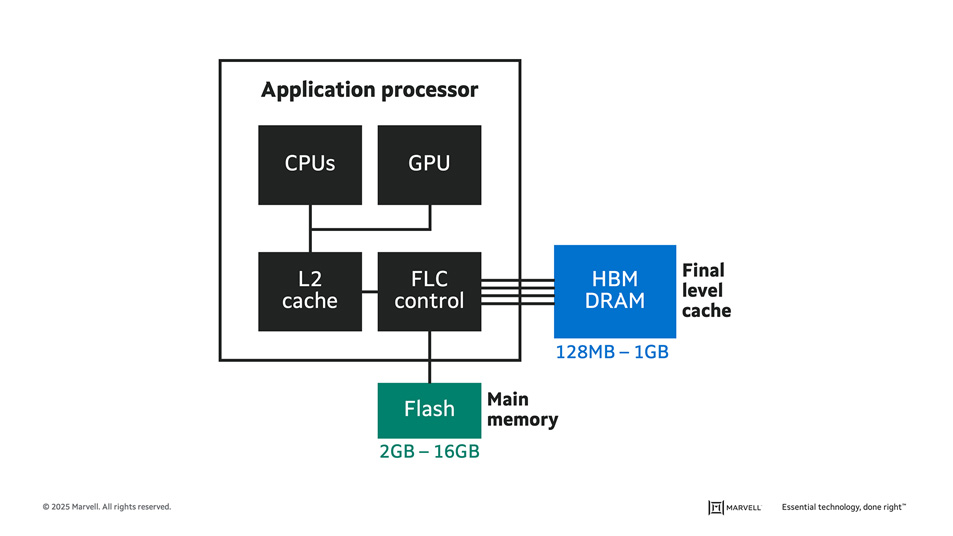
An early MoChi concept combining CPUs, a GPU and a FLC (final level cache) controller for distributing data across flash and DRAM for optimizing power. Credit: Microprocessor Forum.
3. Economics were the driving factor
The primary driver for chiplets revolved around the daunting economics facing chip companies. Chip design costs were rising rapidly. The increase in the number of transistors per chip meant that the number of errors per chip was also rising, potentially leading to lower yields. If the trends continued unabated, it might only make sense in the future to make extremely simple devices, or devices that sold in extremely high volumes.
Chiplets solved a number of problems. Moving away from humongous monolithic devices promised to cut costs and help yields.
Distributing tasks to separate, albeit tightly connected, dies would potentially dampen absolute performance. Nonetheless, it would ameliorate many financial and manufacturing problems.
4. Manufacturing equipment was also a factor
The dimensions of semiconductor equipment—the mask sizes, the sizes of the trays that shuttle devices through the manufacturing process—have remained stable for years—the size of the reticle, or photomask, sits at 858 sq. mm. Rather than design larger reticles for larger chips, it became easier to create packaging and interconnects for stacking dies vertically. Advanced packages today, for instance, can contain 2.8x more silicon than the largest monolithic devices.5
5. Chiplets are outpacing monolithic devices in design starts
New designs based on chiplet principles are growing at a rate of 44% per year, according to data presented by Siemens at the User2User Conference in April 2025. By contrast, monolithic processor design starts are growing at 9%.6
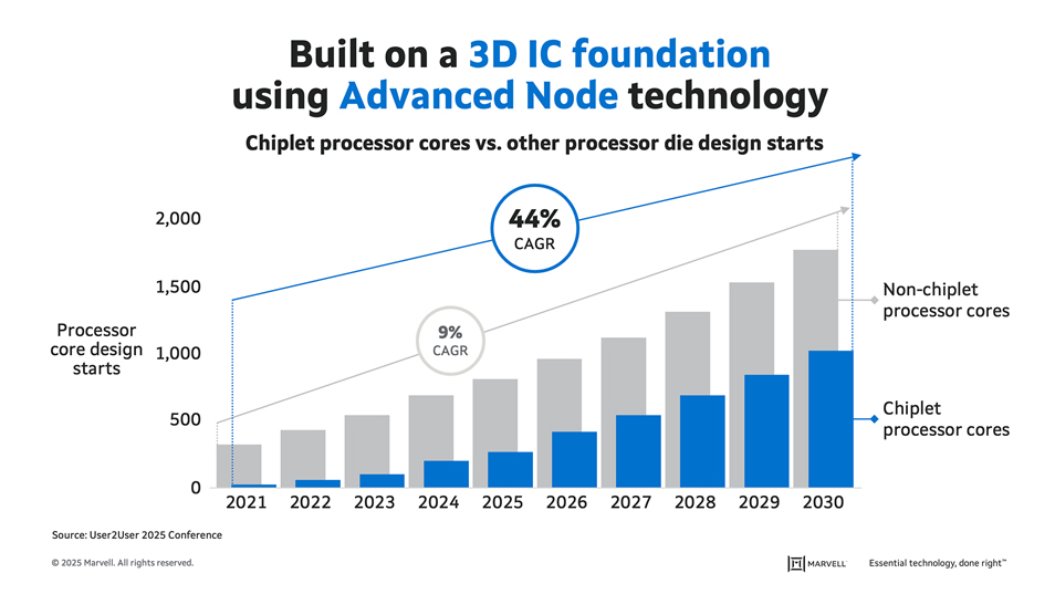
Chiplets will rise from a rounding error in processor design starts to passing monolithic design starts in 2028.
6. Chiplets also win the revenue race
Chiplet revenue is expected to grow from $43.5 billion in 2024 to $144.9 billion in the compute segment 7 and $236 billion overall by 2030, according to TechInsights, thanks to declining costs and advancements in technology.
“Chiplets constitute one of the most dynamic segments of the semiconductor market. We anticipate that chiplet processor revenue will grow by 31% per year,” said James Sanders, senior analyst at the firm.8 “Advanced packaging technologies are critical to the evolution of chiplets, giving designers a framework in which to experiment.”
7. Multi-vendor chiplets are arguably already here
Has anyone come up with a chiplet that contains dies from multiple vendors? It depends on how you look at it. An open ecosystem that lets you assemble chiplets with multiple dies from various vendors—a long-held dream—remains a work in progress.
But look at XPUs and AI accelerators. Chip designers incorporate stacks of high-bandwidth memory from third party memory vendors into the chip package containing computing cores. Thus, devices from two vendors can be found inside most accelerators.
Marvell, meanwhile, is collaborating with leading memory providers to customize the base die and interfaces that link the computing cores to the XPU stacks. That brings the number of vendors inside the computing package to potentially three vendors.
Likewise, custom SRAM—which can reduce overall area by 15% while simultaneously reducing power9—effectively involves combining cores and IP from different companies.
8. Chiplets are opening new frontiers of integration
CPU cores and memory, however, have long been combined. Can chiplets be used to couple discrete parts that usually don’t interact? Yes. Packaged Integrated Voltage Regulator (PIVR) power solutions essentially involve incorporating power semiconductors—usually a discrete chip located on a different part of the motherboard from the computing core—into the chip package. Power semis are typically produced by specialists like Infineon and Empower Semiconductor.
Similarly, chiplets will become a vehicle for directly integrating optics into processors.
9. How high is high? Who knows?
Mayank Mayukh, senior distinguished engineer of advanced packaging at Marvell, says 4D chips containing four layers of devices and 16 times more transistors than monolithic devices are already under discussion in the industry.
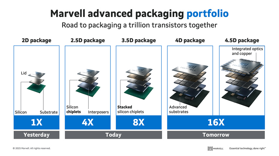
The difference between 2D and 2.5D (or any other number). An interposer serves as both an electrical switch/connectivity platform between chips and a mezzanine/half-step in an advanced package.
10. Will the “System-Let” be next?
To further optimize data centers, chiplet designs will be tightly dovetailed with server, rack and row design. Electronic design automation (EDA) tools for developing cohesive systems will be developed so data center owners can better understand (and compensate for) the interplay of airflow, mechanical stress, power, and other factors across their entire environment.
1. Dave Patterson, IEEE Xplore, March 2006
2. Junko Yoshida, Techsplicit, September 2024
3. Sehat Sutardja, ISSCC, February 2015
4. Linley Gwennap, Microprocessor Report, June 2015
5. Marvell, May 2025
6. Siemens User2User conference; Photo: author
7. TechInsights: Chiplet Market, Compute Segment, 2025; Report Overview, Chiplet Market Introduction, 2025.
8. James Sanders, Marvell press release, May 2025.
9. Marvell, May 2025.
# # #
This blog contains forward-looking statements within the meaning of the federal securities laws that involve risks and uncertainties. Forward-looking statements include, without limitation, any statement that may predict, forecast, indicate or imply future events or achievements. Actual events or results may differ materially from those contemplated in this blog. Forward-looking statements are only predictions and are subject to risks, uncertainties and assumptions that are difficult to predict, including those described in the “Risk Factors” section of our Annual Reports on Form 10-K, Quarterly Reports on Form 10-Q and other documents filed by us from time to time with the SEC. Forward-looking statements speak only as of the date they are made. Readers are cautioned not to put undue reliance on forward-looking statements, and no person assumes any obligation to update or revise any such forward-looking statements, whether as a result of new information, future events or otherwise.
Tags: data centers, AI, AI infrastructure, Optical Interconnect Packaging, chiplet-based SoCs