
By Andrew Yick, Technical Associate Vice President, Operations Engineering, Marvell
This article was first published in Photonic Integrated Circuits magazine.
The dominant challenge in modern AI infrastructure is not just the performance of a single accelerator but scaling up to thousands of accelerators (XPUs) in a cluster. Training and inference workloads now depend on an interconnect that can stitch these accelerators into a high-bandwidth, low-latency system, where performance is governed as much by the network as by the compute itself.
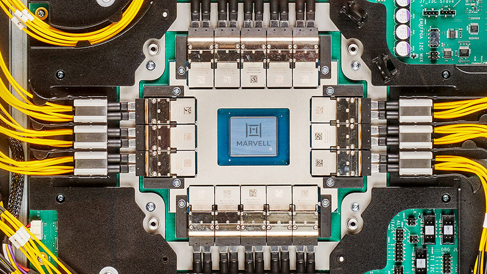
As these systems scale, physics asserts itself. Electrical links over copper hit a practical ceiling as routing density and channel loss collide, turning the loss bandwidth product into an impassable constraint. The choice is binary: either move electrical-to-optical conversion closer to the Application-Specific Integrated Circuit (ASIC) or surrender the link budget. Thus, to bypass this electrical wall, optics must migrate from the board edge and onto the ASIC package.
By Preet Virk, Senior Vice President and General Manager, Photonic Fabric Business Unit
Modern AI infrastructure is built around multi-rack systems where thousands to tens of thousands of accelerators operate as a single logical compute element. As agentic AI and Mixture of Experts (MoE) models accelerate AI adoption, they are driving unprecedented scale and communication demands across data center infrastructure. These systems are connected by scale-up and scale-out networks that must deliver high bandwidth, low latency and efficient power. As these networks extend across racks, maintaining that performance becomes a primary challenge.
As AI systems grow in complexity and scale, the network becomes the backbone of the compute system. Large-scale clusters require massive XPU-to-XPU communication, driving an evolution beyond legacy protocols like PCIe® to encompass UALink™ (Ultra Accelerator Link), ESUN (Ethernet scale-up networking) and NVLink.
Meeting these requirements demands a new approach to connectivity. Marvell provides a comprehensive AI connectivity portfolio spanning scale-up, scale-out, scale-across and DCI (data center interconnect) network architectures. For scale-up networking, Marvell delivers copper and optical interconnects connecting XPUs, switches and memory. Within the rack, Marvell copper solutions provide low-latency, power-efficient short-reach connectivity, while Marvell optical interconnects enable high-performance scaling beyond the rack. This enables XPUs to operate as a more efficient, unified system as scale-up domains expand.
By Vienna Alexander, Marketing Content Professional, Marvell

Marvell was announced as the top Connectivity winner in the 2025 LEAP Awards for its 1.6 Tbps LPO Optical Chipset. The judges' remarks noted that “the value case writes itself—less power, reduced complexity but substantial bandwidth increase.” Marvell earned the gold spot, reaffirming the industry-leading connectivity portfolio it is continually building.
The LEAP (Leadership in Engineering Achievement Program) Awards recognize best-in-class product and component designs across 11 categories with the feedback of an independent judging panel of experts. These awards are published by Design World, the trade magazine that covers design engineering topics in detail.
This chipset, combining a 200G/lane TIA (transimpedance amplifier) and laser drivers, enables 800G and 1.6T linear-drive pluggable optics (LPO) modules. LPO modules offer longer reach than passive copper, at low power and low latency, and are designed for scale-up compute-fabric applications.
By Winnie Wu, Senior Director Product Marketing at Marvell
Welcome to the beginning of row-scale computing.
At the 2025 OCP Global Summit, Marvell and Infraeo will showcase a breakthrough in high-speed interconnect technology — a 9-meter active electrical cable (AEC) capable of transmitting 800G across standard copper. The demonstration will take place in the Marvell booth #B1.
This latest innovation brings data center architecture one step closer to full row-scale AI system design, allowing copper connections that stretch across seven racks - that’s nearly the length of a standard 10-rack row. It builds on the prior achievement by Marvell of a 7-meter AEC demonstrated at OFC 2025, pushing high-speed copper technology even further beyond what was thought possible.
Pushing the Boundaries of Copper
Until now, copper connections in large-scale AI systems have been limited by reach. Traditional electrical cables lose signal quality as distance increases, restricting system architects to a few meters between servers or racks. The 9-meter AEC changes that equation.
By combining high-performance digital signal processing (DSP) with advanced noise reduction and signal integrity engineering, the new design extends copper’s effective range well beyond conventional limits, maintaining clean, low-latency data transfer over distances once thought achievable only with optical fiber.
By Annie Liao, Product Management Director, ODSP Marketing, Marvell
For over 20 years, PCIe, or Peripheral Component Interconnect Express, has been the dominant standard to connect processors, NICs, drives and other components within servers thanks to the low latency and high bandwidth of the protocol as well as the growing expertise around PCIe across the technology ecosystem. It will also play a leading role in defining the next generation of computing systems for AI through increases in performance and combining PCIe with optics.
Here’s why:
PCIe Transitions Are Accelerating
Seven years passed between the debut of PCIe Gen 3 (8 gigatransfers/second—GT/s) in 2010 and the release of PCIe Gen 4 (16 GT/sec) in 2017.1 Commercial adoption, meanwhile, took closer to a full decade2
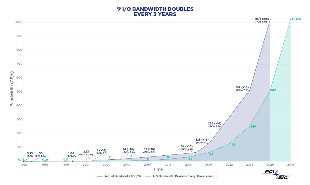
Toward a terabit (per second): PCIe standards are being developed and adopted at a faster rate to keep up with the chip-to-chip interconnect speeds needed by system designers.