By Michael Kanellos, Head of Influencer Relations, Marvell
Chiplets—devices made up of smaller, specialized cores linked together to function like a unified device—have dramatically transformed semiconductors over the past decade. Here’s a quick overview of their history and where the design concept goes next.
1. Initially, they went by the name RAMP
In 2006, Dave Patterson, the storied professor of computer science at UC Berkeley, and his lab published a paper describing how semiconductors will shift from monolithic silicon to devices where different dies are connected and combined into a package that, to the rest of the system, acts like a single device.1
While the paper also coined the term chiplet, the Berkeley team preferred RAMP (Research Accelerator for Multiple Processors).
2. In Silicon Valley fashion, the early R&D took place in a garage
Marvell co-founder and former CEO Sehat Sutardja started experimenting with combining different chips into a unified package in the 2010s in his garage, according to journalist Junko Yoshida.2 In 2015, he unveiled the MoChi (Modular Chip) concept, often credited as the first commercial platform for chiplets, in a keynote at ISSCC in February 2015.3
The first products came out a few months later in October.
“The introduction of Marvell’s AP806 MoChi module is the first step in creating a new process that can change the way that the industry designs chips,” wrote Linley Gwennap in Microprocessor Report.4
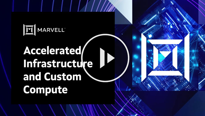
An early MoChi concept combining CPUs, a GPU and a FLC (final level cache) controller for distributing data across flash and DRAM for optimizing power. Credit: Microprocessor Forum.
By Michael Kanellos, Head of Influencer Relations, Marvell
More customers, more devices, more technologies, and more performance—that, ultimately, is where custom silicon is headed. While Moore’s Law is still alive, customization is taking over fast as the engine for driving change, innovation and performance in data infrastructure. A growing universe of users and chip designers are embracing the trend and if you want to see what’s at the cutting edge of custom, the best chips to study are the compute devices for data centers, i.e. the XPUs, CPUs, and GPUs powering AI clusters and clouds. By 2028, custom computing devices are to account for $55 billion in revenue, or 25% of the market.1 Technologies developed for this segment will trickle down into others.
Here are three of the latest innovations from Marvell:
Multi-Die Packaging with RDL Interposers
Achieving performance and power gains by shrinking transistors is getting more difficult and expensive. “There has been a pretty pronounced slowing of Moore’s Law. For every technology generation we don’t get the doubling (of performance) that we used to get,” says Marvell’s Mark Kuemerle, Vice President of Technology, Custom Cloud Solutions. “Unfortunately, data centers don’t care. They need a way to increase performance every generation.”
Instead of shrinking transistors to get more of them into a finite space, chiplets effectively allow designers to stack cores on top of each other with the packaging serving as the vertical superstructure.
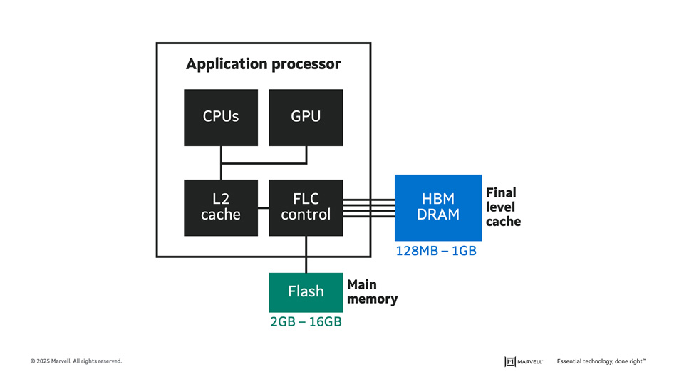
2.5D packaging, debuted by Marvell in May, increases the effective amount of compute silicon for a given space by 2.8 times.2 At the same time, the RDL interposer wires them in a more efficient manner. In conventional chiplets, a single interposer spans the floor space of the chips it connects as well as any area between them. If two computing cores are on opposite sides of a chiplet package, the interposer will cover the entire space.
Marvell® RDL interposers, by contrast, are form-fitted to individual computing die with six layers of interconnects managing the connections.
2.5D and multilayer packaging. With current manufacturing technologies, chips can achieve a maximum area of just over 800 sq. mm. By stacking them, the total number of transistors in an XY footprint can grow exponentially. Within these packages, RDL interposers are the elevator shafts, providing connectivity between and across layers in a space-efficient manner.
By Radha Nagarajan, SVP and CTO, Optical and Copper Connectivity Business Group
The exponential increase in bandwidth demand will drive continuous innovation in, and deployment of, data movement interconnects for Cloud and Telecom providers. As a result, highly integrated silicon photonics platform solutions are expected to become a key enabling technology for the cloud and telecom market over the next decade.
What Does Highly Integrated Silicon Photonics Platform Mean for the Infrastructure Business?
As speed continues to go up, optical will replace copper as the primary conduit of the digital bits inside Cloud data centers. Marvell is investing heavily in silicon photonics to complement our high-speed CMOS technologies in data center interconnects to accelerate this transition.